


Advertisement
Nvidia's GTC 2024 in-house trade fair in San José, California, took place in person for the first time in years and was, unsurprisingly, all about artificial intelligence. With its accelerator chips, Nvidia currently dominates the market for data centers and is generating one financial record result after another in the wake of the AI boom.
Nvidia boss Huang wants it to stay that way. The newly introduced Blackwell accelerator architecture plays the central role in the form of various products that are scheduled to come onto the market over the course of the year, from the B100 to the DGX GB200 SuperPOD. On paper, Blackwell GPUs achieve twice the throughput on some data formats compared to AMD's brand new MI300 accelerators.
With the new Blackwell architecture and further reduced data formats such as 4-bit floating point as well as new functions, the focus is primarily on energy efficiency and data exchange between the individual chips. That's why the NVLink switch and the network technology have also been upgraded.

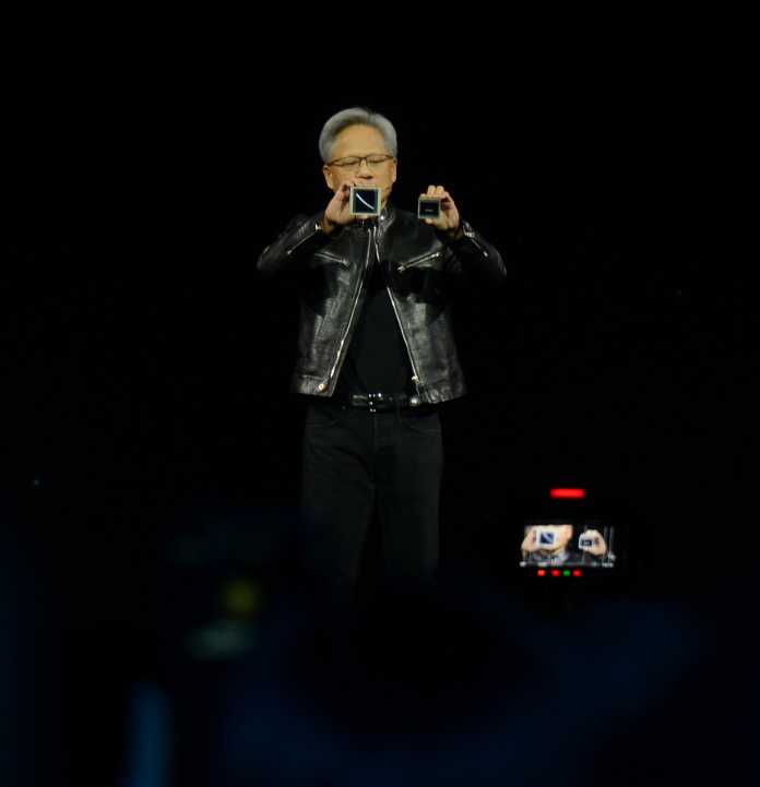
Nvidia boss Huang holds Blackwell (left) and Hopper (right) into the camera.
(Image: c't)
Nvidia traditionally does not name prices and refers to its partners, but as long as the AI hype continues unabated, the chips are likely to sell almost regardless of the pricing. In any case, Nvidia has already won Amazon Web Services, Google Cloud and Oracle Cloud as customers, but does not specify exactly when instances will be available to book. Meanwhile, the older H100 products continue to roll off the production line.
Blackwell-Doppelchip
Nvidia is breaking new ground with Blackwell, but in some ways remains true to itself. The Blackwell “GPU” consists of two individual chips. Nvidia did not want to answer our question as to whether the two are functionally identical, but stated that both reach the limit of the exposure options. This means that they should each be around 800 mm² in size and therefore occupy approximately as much space individually as the predecessors H100 (814 mm²) and A100 (826 mm²). The word chiplet was not mentioned, as it is usually understood to mean the coupling of different chips.
Nvidia has the Blackwell chips manufactured at TSMC in a process called “4NP”, which does not correspond to the manufacturer's usual nomenclature. Nvidia did not answer whether this is a derivative of N4P or what characteristics the process has – but we assume that it is N4P, in which, as usual, a few parameters were adjusted according to customer requirements.
Both chips, which Nvidia only calls the Blackwell GPU, are connected to each other via a fast interface with 10 TBytes per second (5 TBytes/s in each direction). According to Nvidia, this is enough for them to behave like a single GPU in terms of performance. For comparison: With the level 2 cache as the data connecting instance in Nvidia's high-end GeForce RTX 4090 graphics cards, we measured around 5 TBytes per second, AMD's MI300 accelerator chiplets are connected to each other at up to 1.5 TBytes/s.
192 GB HBM3e memory
When it comes to memory, Nvidia is going all out and is starting with eight 24 GB stacks of fast HBM3e memory. A total of up to 192 GB and 8 TB/s transfer rate comes together. In terms of memory size, the company is on par with AMD's MI300X, but the B100 has a transfer rate that is around 50 percent higher – the upgrade was also necessary because Nvidia's H100 generation was lagging behind, especially when it came to memory size. With eight stacks, you theoretically also have the option of later switching to a 36 GB stack and increasing the capacity to 288 GB.
There were only a few details about the internal structure at the presentation. Nvidia only gave performance data for the Tensor cores, but remained silent about traditional shader calculators and other units.
For the presentation in the table we used the throughput values with sparsity; with densely populated matrices the teraflops figures are halved.
| Accelerators for data centers and AI | ||||
|
Name |
GB200 |
AMD MI300X |
H100 |
A100 |
|
architecture |
1x Grace + 2x Blackwell |
CDNA3 |
Hopper |
Ada |
|
Transistors |
2x 10⁴ Mrd. / 4NP / ~800 mm² |
Various chiplets with 153 billion / N5 + N6 |
80 Mrd. / 4N / 814 mm² |
54,2 Mrd. / N7 / 826 mm² |
|
Format |
Add-on-Board (2 pro 1U-Rack) / SXM |
SXM5 |
SXM5 |
SXM4 |
|
Year |
2024 |
2023 |
2022 |
2020 |
|
TDP |
1200 Watt |
750 Watt |
700 Watt |
400/500 Watt |
|
Storage |
192 GB HBM3e |
192 GB HBM3 |
80 GB HBM3 |
80 GB HBM2E |
|
Transferrate |
8 TByte/s |
5.3 TByte/s |
3.35 TByte/s |
2.04 TByte/s |
|
GPU-GPU connection |
NVLink Gen 5, 1,8 TByte/s |
896 GByte/s |
NVLink Gen 4, 900 GB/s |
NVLink Gen 3, 600 GB/s |
|
Computing power Tensor core via GPU (TFLOPS, with sparsity) |
||||
|
FP64 (Teraflops) |
45 |
163 |
67 |
19,5 |
|
FP32 (Teraflops) |
k.Information |
163 |
k. specification |
k. specification |
|
TF32 (Teraflops) |
2500 |
1307 |
989 |
312 |
|
BF16 (Teraflops) |
5000 |
2615 |
1979 |
624 |
|
FP8 (Teraflops) |
10000 |
5230 |
3958 |
k. Specification (INT8: 1248 TOPS) |
|
FP4 (Teraflops) |
20000 |
k.Information |
k. specification |
k. specification |
|
Computing power shader cores per GPU (teraflops) |
||||
|
FP64 (Teraflops) |
k.Information |
81,7 |
33,5 |
9,7 |
|
FP32 (Teraflops) |
k.Information |
163,4 |
66,9 |
19,5 |
|
BF16 (Teraflops) |
k.Information |
k.Information |
133,8 |
39 |
|
FP16 (Teraflops) |
k.Information |
k.Information |
133,8 |
78 |
FP4 and FP6
New to Blackwell is, among other things, support for a 4-bit floating point format (FP4), for which there is a research paper with the collaboration of an Nvidia employee, in the chip's Transformer engine. This means that weights and activations for AI inferencing of Large Language Models (LLM) should be saved with just 4 bits. The authors claim “Our method can quantize both the weights and activations in the LLaMA-13B model to just 4 bits for the first time and achieves an average score of 63.1 on the common-sense zero-shot reasoning tasks , which is only 5.8 points lower than the full-precision model and significantly exceeds the previous state of the art by 12.7 points.” FP4 could therefore handle significantly less data with only relatively small losses in the accuracy of the result, which not only doubles the processing speed but also doubles the possible model size.
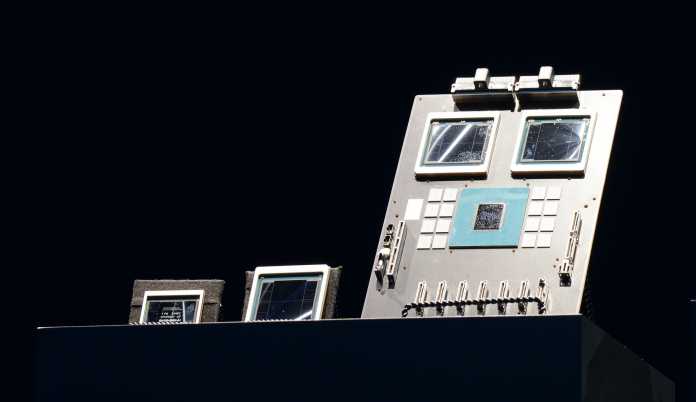
The Blackwell exhibits right and center in the picture: GB200 board and Blackwell double chip
(Image: c't)
Update: During the keynote, Nvidia CEO Huang also revealed that FP6 is also an option. This format does not provide additional computing throughput compared to FP8, but it saves memory, cache and register space and therefore also energy.
With a GPT model with 1.8 trillion parameters (English: “1.8T Params”), Nvidia wants to be 30 times as fast as an H100 with a GB200 with a so-called Mixture of Experts, i.e. adjusted calculation and data accuracy. based system and work 25 times more efficiently. Nvidia claims to have reduced the performance to one GPU, but in reality it compares a system with 8 HGX100 and 400G Infiniband interconnect with 18 GB200 superchips (NVL36).
But even with the established FP8 data format, Blackwell is on paper almost twice as fast as AMD's MI300X and more than 2.5 times as fast as its predecessor H100.
